

This post is the second in a series about how to read CT scans, in collaboration with Lumafield (which provided our awesome CT scanner) and No Starch Press (which contributed all the cool cross-section images from the book Open Circuits). In Part 1, we ran through the basics of what a CT scanner is, how it works, and how it can be invaluable for teardowns and repairs.
For anyone just joining this Computed Axial Tomography or CT scan party, a brief recap:
If you’ve ever had a CT scan at a hospital, you basically know the drill: These fancy X-ray machines create hundreds or thousands of X-ray slices and stitch them back together with software to create a 3D model of something’s insides. A doctor might use the resulting image to diagnose a broken bone or a blood clot.
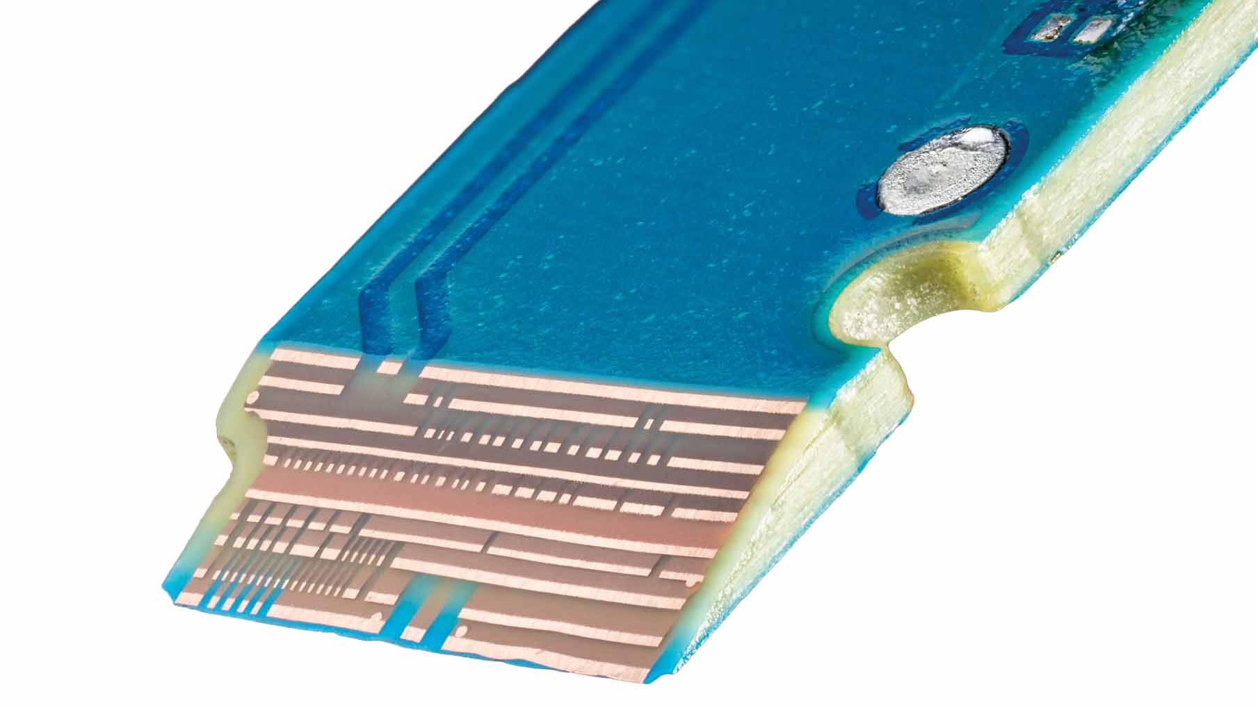
For repair, we don’t really use it the same way: you could diagnose a broken solder joint or a blown capacitor with CT, but since a scan takes many hours in a huge expensive machine, that’s not realistic for most repairs. Instead, we use CT long before repair is even necessary, to help us figure out where everything is inside a device. It tells us whether there are hidden screws or clips, how components fit inside something that’s totally sealed, and what path traces take inside a many-layer PCB. Think of it as a high-resolution map for a repair detective. We share our scans with you so that you can use them to figure out repairs we don’t yet have guides for. (And because they’re just so cool.)
But before you can make sense of a CT scan of a whole device, it helps to know what some common components look like and how their technicolor CT shapes compare to what you’d see with your real actual eyes. So feast those eyes below, on CT scans paired up with cross-section images—with thanks again to Lumafield and No Starch Press.
Electrolytic Capacitors
Through-hole electrolytic capacitors, with their long cylindrical structures, are one of the easier-to-spot components on a PCB, though you’ll only see them in larger electronics like TVs. Regardless of what they’re made of and what they look like, the function of a capacitor remains the same: to store and release energy.
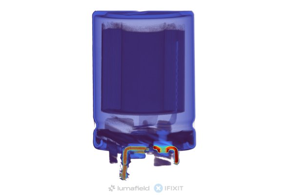
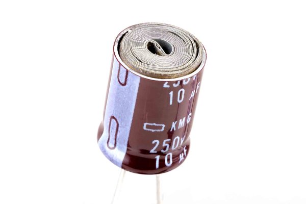
Electrolytic capacitors, like the ones pictured here, consist of two conductive aluminum foils (anode and cathode) separated by an electrolyte-soaked paper. The anode foil has an oxide layer that acts as the dielectric. In CT scans, you’ll spot their cylindrical shape with a metal can housing, often topped with a pressure vent. Cross-sections reveal the spirally-wound foils and paper separator, while CT images highlight density differences between the metal housing, aluminum foils, and electrolyte-filled spaces.
But you can’t fit a through hole component into smaller electronic devices, so you’re far more likely to see Surface Mount Device (SMD) tantalum capacitors instead. Tantalum is a conflict metal that, while classified as a rare metal, is not technically rare as much as it is in high demand and dirty to extract. Over 40% of the worlds tantalum is sourced from coltan mining in the DRC, where conflict, child labor, and environmental concerns have brought to the fore the need to recycle and reuse the tantalum that’s already in circulation in our devices.
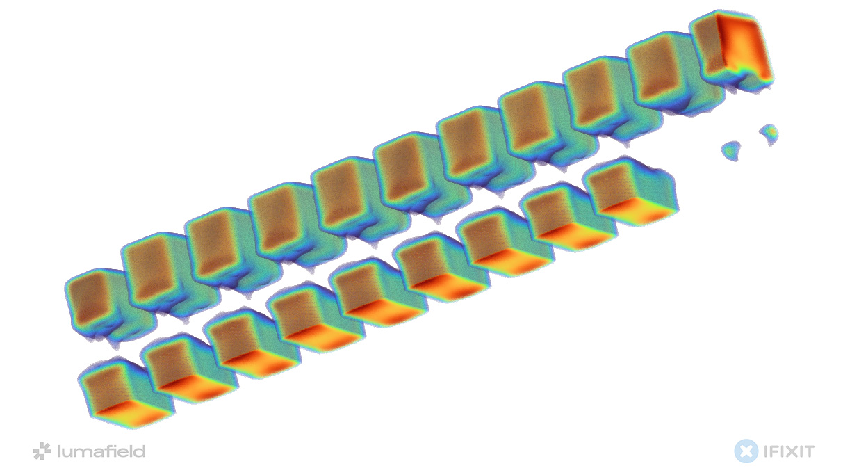
There’s no question though, our modern lives are highly dependent on tantalum capacitors and there really isn’t any meaningful alternative available. Their size, relative capacitance, stability under varied temperature ranges, and long life make them ideal for delivering smooth voltages to highly sensitive ICs while filtering noise in circuits.
Tantalum is a very dense material and can usually be spotted fairly easily in X-rays. In this example, a line of capacitors near the NAND flash IC of a Mac Mini storage module (bottom right) collectively provide a steady voltage and filter noise emanating from the inductor directly adjacent. The density of the two larger components nearby reveals two polymer electrolytic capacitors (top left, note the size).
Transformers
The vast majority of your household electronics run on voltages that are far below the 120V (or 100V to 240V depending on where in the world you live) you get from the wall socket. If you take a look at your laptop adaptor, it will have a label that says something along the lines of “Input: 120-240V…” and “Output: 15-36V…”. Manipulating (stepping-up or stepping-down) voltage is what transformers do.
Both the CT and cross-section images show the primary and secondary coils wound around a ferromagnetic core, with no direct electrical connection between them. When alternating current flows through the primary coil (the thicker copper wires in the cross section), it creates a changing magnetic field that induces a voltage in the secondary coil (the thinner copper wires). The voltage in the secondary coil is determined by the number of copper windings in that coil.
Transformers come in various sizes, from hefty fist-sized components like the ones pictured above to tiny thumbnail sized components found in laptop and cellphone GaN chargers.
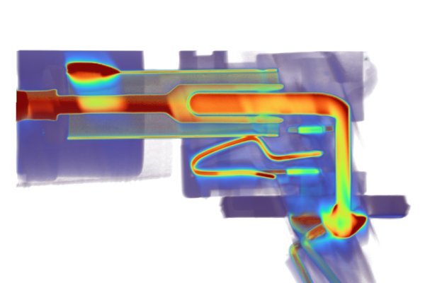
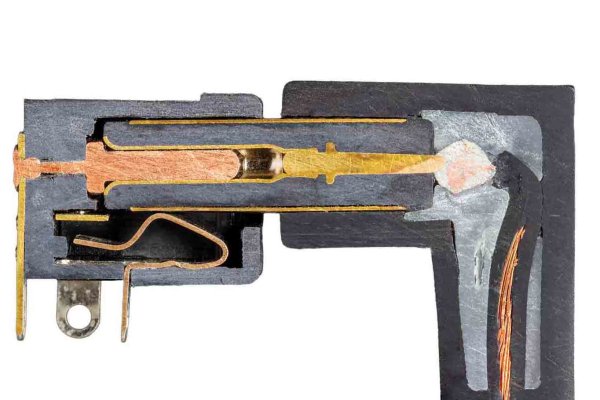
Barrel Plug & Jack
USB-C might be slowly taking over the world but barrel connectors still form the backbone of power delivery to most electronics and household appliances. They are exceedingly simple to understand once you strip away the outer layers, consisting of an inner pin and outer sleeve separated by insulation. In most instances you’ll find that the center pin is positive and the outer sleeve is negative but there are plenty of exceptions to this rule so it’s worth confirming compatibility before plugging in any random adapter into a device.

In CT scans, barrel jack connectors appear as cylindrical structures with hollow sections. Cross-sections reveal the conductive paths and contact mechanisms, while CT images show the different metal densities of inner and outer conductors, insulating materials, and spring contacts that ensure reliable connections. The design prevents accidental shorts while maintaining consistent power delivery.
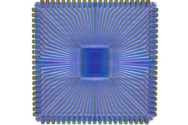
Ball Grid Array (BGA)
Ball Grid Arrays are advanced chip packaging methods where components connect to circuit boards via an array of solder balls on the underside. Unlike traditional pins, these balls create both electrical connections and mechanical mounting.
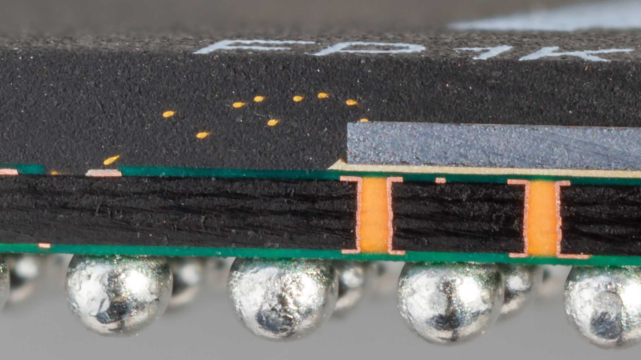
In CT scans, BGAs appear as a grid of regularly-spaced dense spots beneath rectangular packages. Cross-sections reveal the component body, substrate layers, and hemispherical solder connections, while CT images show the uniform spacing pattern of solder balls and internal porosity that may result from reflow soldering.
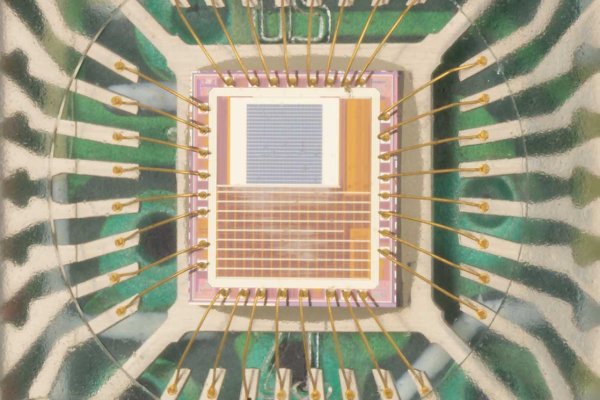
Microcontrollers
Microcontrollers are compact computers-on-a-chip containing a processor core, memory, and programmable input/output peripherals. They serve as the “brains” of embedded systems, running software to control device functions. Some microcontrollers, like the one pictured below, are designed to be UV erasable and incorporate a clear crystal window directly over the die giving us an unobstructed view of the silicon die and the bonding wires connecting to package leads.
A CT scan of a microcontroller provides further visual insight into how those bonding wires expand to far sturdier surface contact points.
Cathode Ray Tube (CRT)
CRT’s may be considered obsolete in the consumer space but that doesn’t make the technology any less interesting. CRT displays work by firing electron beams from a heated cathode toward a phosphor-coated screen. Electromagnetic coils deflect these beams to create images. The CT scan on the left shows a CRT pulled from an old Phillips oscilloscope comprising of a large glass structure with distinctive neck and funnel regions. The cross-section on the right reveals the electron gun assembly, deflection coils, and vacuum space, while CT images highlight the varying glass thickness, dense metal components, and internal support structures designed to withstand atmospheric pressure on the vacuum inside.
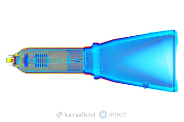
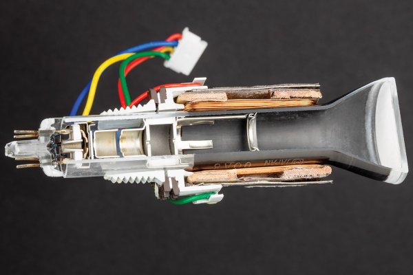
3.5MM Jack
The 3.5mm TRS (Tip, Ring, Sleeve) audio plug connects headphones, speakers, and microphones to any device with a headphone jack.


TRS plugs use cylindrical metal contacts of different lengths to carry audio signals, with up to three contacts for stereo audio plus microphone. You can also get TRRS plugs (Tip, Ring, Ring, Sleeve) that add a fourth contact point commonly used for combining stereo audio with microphone functionality in a single connector.
But that’s not all TRS can do! With some clever engineering, a TRS plug can also be used to deliver power as in the case of the 100W capable iFixit Smart Soldering Iron tips.
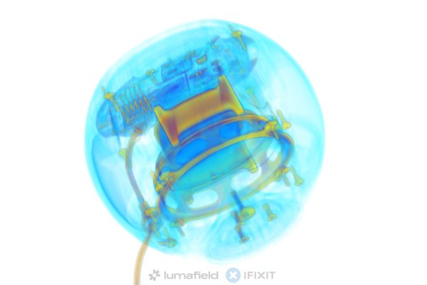
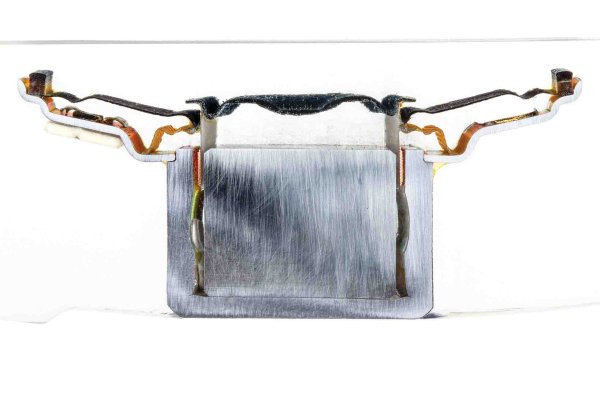
Speakers
Speakers convert electrical signals into sound waves through electromagnetic induction. A current-carrying coil placed in a magnetic field moves a diaphragm to create sound pressure waves. The copper coil can be seen in this cross section wrapping it’s way between the two metal blocks that form the base of the speaker. A CT scan of the HomePod Mini shows a very similar speaker that dominates the interior of the device.
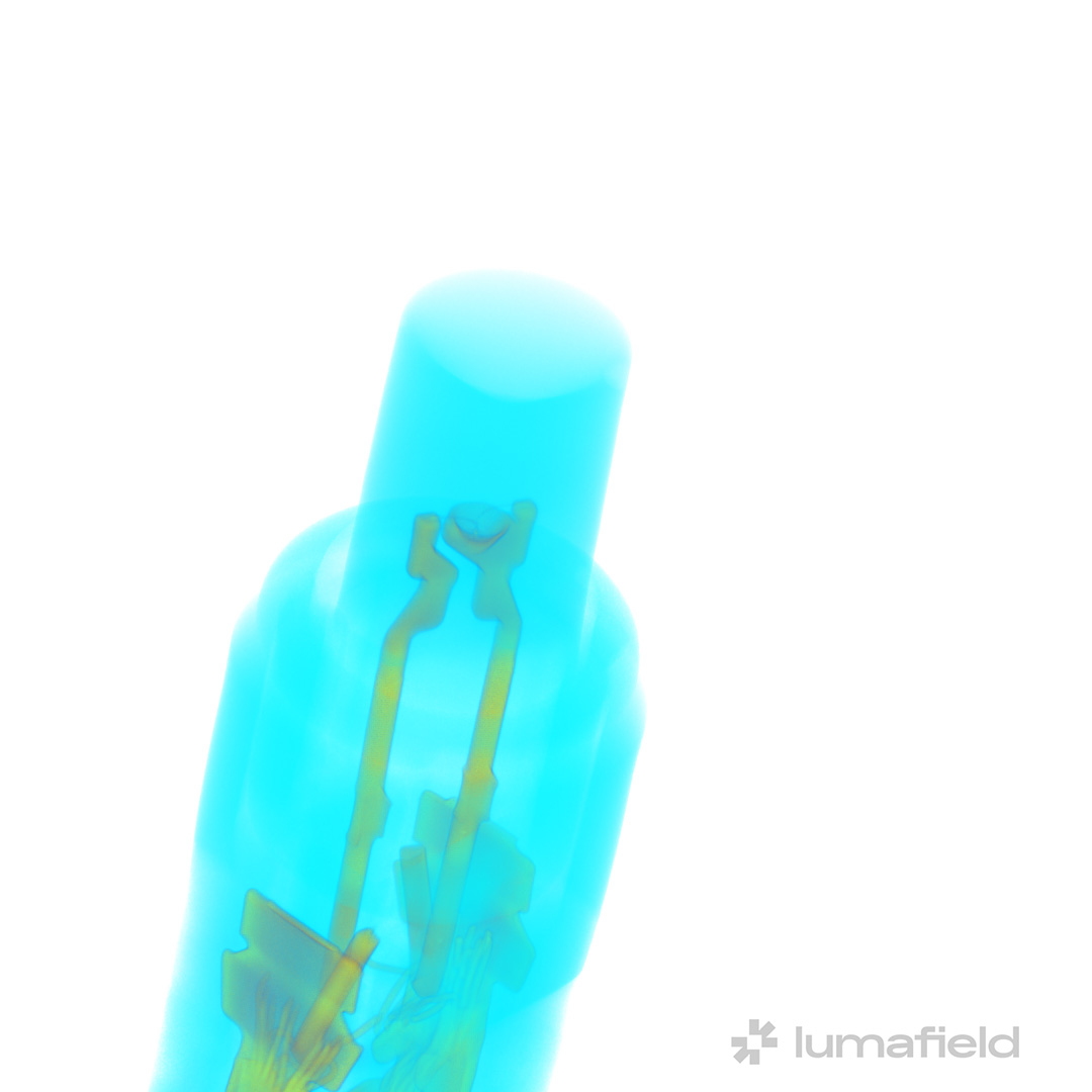
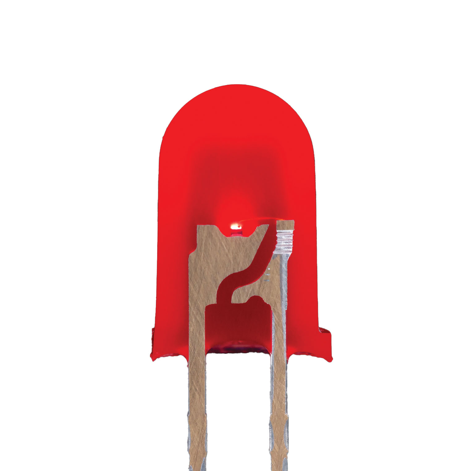
Light Emitting Diodes (LEDs)
LEDs convert electrical energy directly into light through electroluminescence. When forward-biased, electrons recombine with holes in the semiconductor, releasing energy as photons. In CT scans, LEDs appear as small components with distinctive internal structures. Cross-sections show the semiconductor die, wire bonds, reflective cup, and lens assembly, while CT images highlight the density differences between the semiconductor material, metal conductors, and plastic encapsulation that shapes the light output.
Lithium Ion Batteries
Last but not least, let’s take a look at the ubiquitous lithium ion battery. These batteries have been instrumental in facilitating the proliferation of portable electronics with cheap, high density energy storage. We’ll talk more about the different types of batteries in Part 3 of this series. For now, suffice to say that the jellyroll structure of lithium polymer batteries (a type of lithium ion battery) can easily be distinguished from both cross-section and CT imagery.
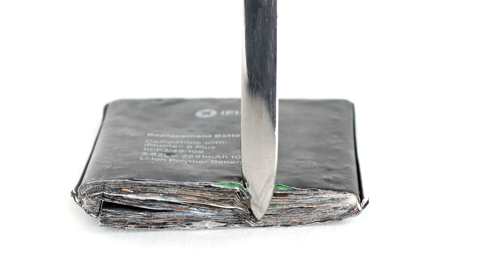
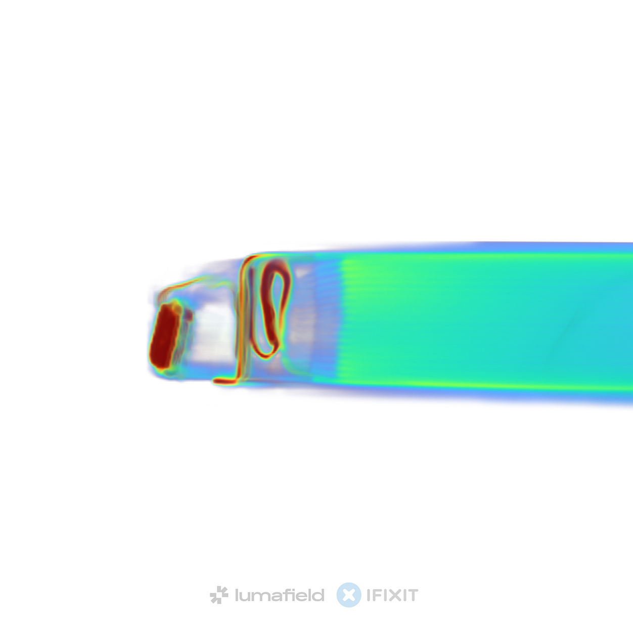
The jellyroll structure is designed to increase the maximum surface area for electrochemical reactions to occur, thereby increasing energy density, but it is a continuous sheet of conductive material that’s rolled up on itself with a cathode and an anode at each end.
Current generation phones have moved away from jellyroll structures in favor of stacked-cell chemistry: multiple single layers are packed on top of each other and are individually connected to a cathode and anode. This reduces the risk of accidental shorts occurring due to cracked or damaged layers touching at the fold points of a jellyroll while also increasing the rate at which the battery can charge and discharge energy.

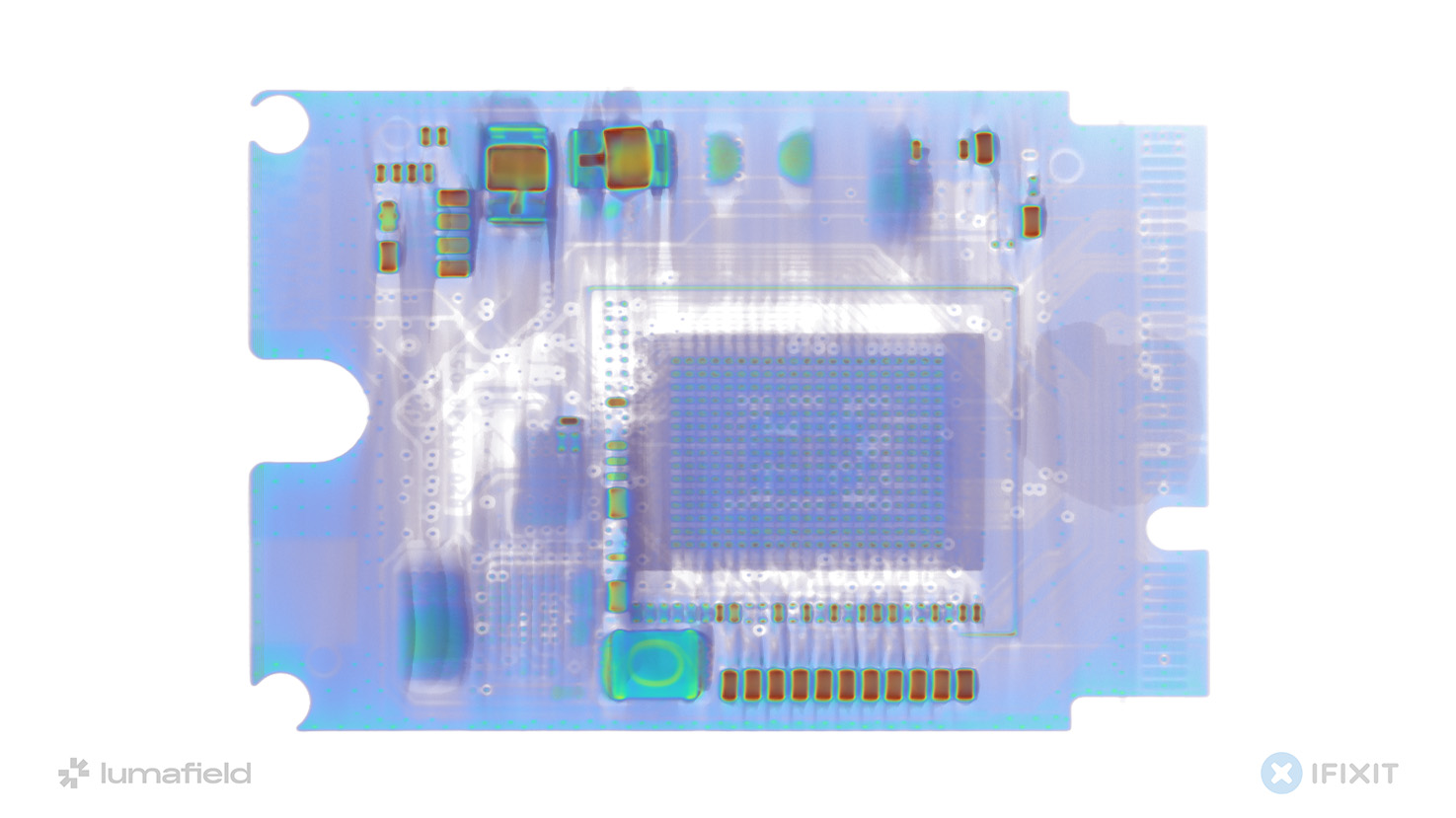
Putting It All Together
Now that you’ve seen what various individual components look like, how about trying your hand at finding some of those components in a Polaroid camera? You won’t find everything we looked at in this blog post, but you can find the following components in the Polaroid Flip:
- Electrolytic capacitor
- Transformer
- Lithium polymer battery
- A sonar transducer (which isn’t a speaker, but behaves like one!)
- Surface mount LED
- BGA solder points
- Microcontrollers
Some of these components will be harder to find than others, but it’s definitely possible with a bit of sleuthing! Think like an engineer. Which component would need a transformer to step-up voltage from a lithium polymer battery?
Hint: you can use the perspective view in the top right-hand corner of the viewport to switch from 3D to the X, Y, or Z-axis and scrub through the layers.
The fun doesn’t stop here. We looked at individual components in Part 2, but for Part 3 we’ll zoom out and consider some common structures that can be identified in CT scans at the macro level. In the meantime, feel free to explore the numerous scans we’ve published alongside our teardowns on iFixit.com.


crwdns2944067:00crwdne2944067:0