crwdns2935425:013crwdne2935425:0
crwdns2931653:013crwdne2931653:0


-
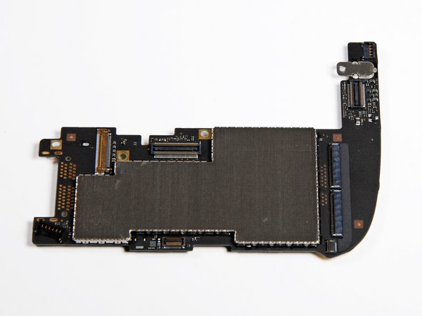
Top and bottom of logic board with the EMI shield on.
-
It looks like this board was made by AT&S. We haven't seen Apple's PCB manufacturers brand their boards before.
-
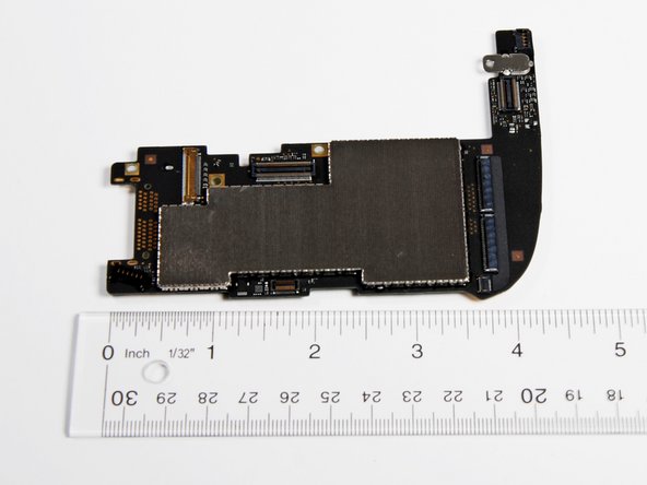
The logic board is about 4.5" wide, spanning about 60% of the iPad's width.
| [* black] Top and bottom of logic board with the EMI shield on. | |
| - | [* black] It looks like this board was made by |
| + | [* black] It looks like this board was made by AT&S. We haven't seen Apple's PCB manufacturers brand their boards before. |
| [* black] The logic board is about 4.5" wide, spanning about 60% of the iPad's width. |
crwdns2944171:0crwdnd2944171:0crwdnd2944171:0crwdnd2944171:0crwdne2944171:0