crwdns2935425:04crwdne2935425:0


-
Screen labelled "NFP200H-20A", could not identify further. Probably some standard TFT display with SPI/I2C.
-
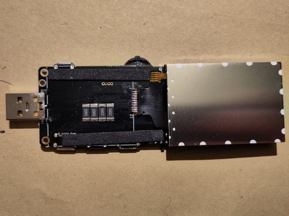
Backside main PCB:
-
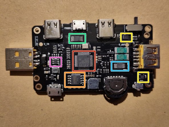
Red square: Artery AT32F403A CGT7 (Main microcontroller) with orange square: W25Q128JV (128M-bit Serial Flash Memory with uniform 4KB sectors and Dual/Quad SPI)
-
Blue square: 3PEAK TPA626 TPA626 (Bi-Directional Current and Power Monitor)
-
Green square: RS2228 MCO7117 (High-Speed USB 2.0 (480-Mbps) 1:2 Multiplexer/Demultiplexer Switch). Probably to switch between the USB micro and -C inputs.
-
Pink square: IC labelled IV7NS. I think it might be a MPS MP2451DT step-down converter. Probably to always provide the 3.3V logic-level voltage for the ICs.
-
Yellow squares: could not identify. One (presumably) QFN14 labelled "UAAC CEH" and one with unknown form factor "WL5 J3".
-
Bluetooth board: pogo-pins to make contact to main board and Tuya BEKEN BK3432
crwdns2944171:0crwdnd2944171:0crwdnd2944171:0crwdnd2944171:0crwdne2944171:0