crwdns2933423:0crwdne2933423:0

Samsung Galaxy Watch3 Teardown

crwdns2936315:0crwdne2936315:0
crwdns2936325:0crwdne2936325:0
crwdns2931653:05crwdne2931653:0
Samsung Galaxy Watch3 Teardown: crwdns2935265:00crwdnd2935265:01crwdnd2935265:03crwdne2935265:0 Samsung Galaxy Watch3 Teardown: crwdns2935265:00crwdnd2935265:02crwdnd2935265:03crwdne2935265:0 Samsung Galaxy Watch3 Teardown: crwdns2935265:00crwdnd2935265:03crwdnd2935265:03crwdne2935265:0
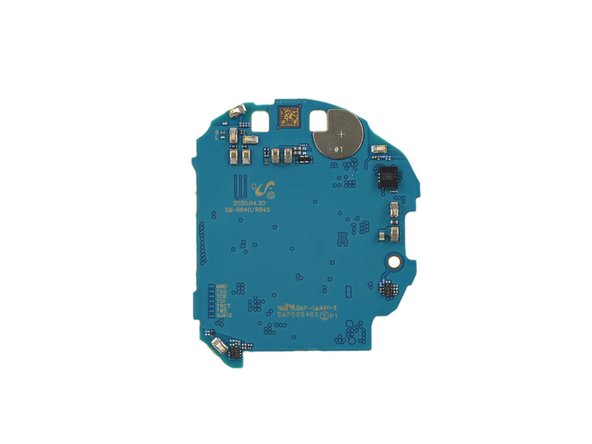
  • Scooping out this vaguely disc-shaped motherboard next, we peek under the shields and find:

  • A Samsung SiP FO-PLP combining the Exynos 9110 dual-core, 1.15 GHz Cortex-A53 processor, their in-house 1 GB DRAM and Power Management IC

  • The SiP FO-PLP stands for System-in-Package Fan-Out Panel Level Packaging and is Samsung’s take on getting as much tech in the tiniest package—which was already used in the original Galaxy Watch.

  • Samsung Shannon 915 Intermediate Frequency IC

  • NXP PN80T NFC controller w/ Secure Element

  • Broadcom BCM430132 WiFi/Bluetooth module and Broadcom GNSS Location Hub for GPS/GLONASS/etc

  • Qualcomm Atheros QPA5580 Power Amplifier (likely)

  • IDT P9222S wireless power receiver

crwdns2935429:0crwdne2935429:0

crwdns2935429:0crwdne2935429:0

crwdns2935429:0crwdne2935429:0

crwdns2935429:0crwdne2935429:0

crwdns2935429:0crwdne2935429:0

crwdns2935429:0crwdne2935429:0

crwdns2935429:0crwdne2935429:0

crwdns2935429:0crwdne2935429:0

crwdns2944171:0crwdnd2944171:0crwdnd2944171:0crwdnd2944171:0crwdne2944171:0