crwdns2933423:0crwdne2933423:0

Samsung Galaxy S9の分解

crwdns2936315:0crwdne2936315:0
crwdns2936323:0crwdne2936323:0
crwdns2931653:06crwdne2931653:0
Samsung Galaxy S9 Teardown: crwdns2935265:00crwdnd2935265:01crwdnd2935265:03crwdne2935265:0 Samsung Galaxy S9 Teardown: crwdns2935265:00crwdnd2935265:02crwdnd2935265:03crwdne2935265:0 Samsung Galaxy S9 Teardown: crwdns2935265:00crwdnd2935265:03crwdnd2935265:03crwdne2935265:0
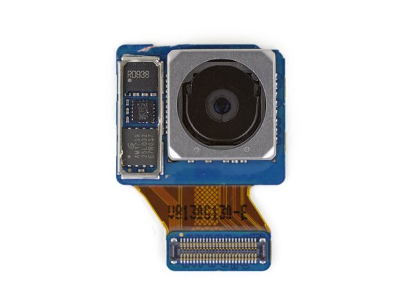
  • Compared to some flagships, the S9 has twice the f-stops and half the sensors.

  • Not shown: Samsung's highly touted 2 Gbit LPDDR4 DRAM, layered right underneath the image sensor.

  • Shown: Some other mystery chips.

  • RD938 likely OIS driver

  • STMicroelectronics L2G2IS 2-axis OIS gyroscope

  • GigaDevice GD25LQ32 32 Mb serial flash

他の最新モデルと比べるとS9はFストップ(絞り値)が倍、センサは半分です。

画像に含まれていないもの:Samsungが売り出し中の2 Gbit LPDDR4 DRAM、画像センサの下に積層されています)

画像中:幾つかのミステリーなチップがあります。

RD938、おそらくOISドライバー

STMicroelectronics L2G2IS 2軸OISジャイロスコープ

GigaDevice GD25LQ32 32 Mbシリアルフラッシュ

crwdns2944171:0crwdnd2944171:0crwdnd2944171:0crwdnd2944171:0crwdne2944171:0